- 您现在的位置:买卖IC网 > Sheet目录2006 > LTC2498IUHF#TRPBF (Linear Technology)IC ADC 24BIT 16CH 38-QFN
LTC2498
34
2498ff
applications inForMation
mode rejection of line frequencies. The common mode
rejectionoflinefrequenciesremainsunchanged,thusfully
differential input signals with a high degree of symmetry
on both the IN+ and IN– pins will continue to reject line
frequency noise.
An increase in fEOSC also increases the effective dynamic
input and reference current. External RC networks will
continue to have zero differential input current, but the
time required for complete settling (580ns for fEOSC =
307.2kHz) is reduced, proportionally.
Once the external oscillator frequency is increased above
1MHz(amorethan3xincreaseinoutputrate)theeffective-
ness of internal auto calibration circuits begins to degrade.
This results in larger offset errors, full scale errors, and
decreased resolution, see Figures 31 to 38.
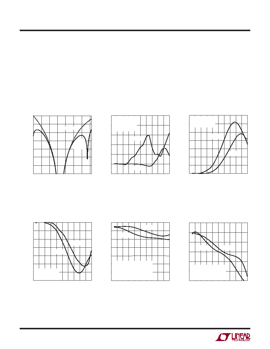
Figure 30. Input Normal Mode Rejection
2x Speed Mode with and Without Running
Averaging
Figure 31. Offset Error vs Output Data
Rate and Temperature
Figure 32. +FS Error vs Output Data
Rate and Temperature
Figure 33.–FS Error vs Output Data Rate
and Temperature
Figure 34. Resolution (NoiseRMS ≤ 1LSB)
vs Output Data Rate and Temperature
Figure 35. Resolution (INLMAX ≤ 1LSB)
vs Output Data Rate and Temperature
DIFFERENTIAL INPUT SIGNAL FREQUENCY (Hz)
48
–70
–80
–90
–100
–110
–120
–130
–140
54
58
2498 F30
50
52
56
60
62
NORMAL
MODE
REJECTION
(dB)
NO AVERAGE
WITH
RUNNING
AVERAGE
OUTPUT DATA RATE (READINGS/SEC)
–10
OFFSET
ERROR
(ppm
OF
V
REF
)
10
30
50
0
20
40
20
40
60
80
2498 F31
100
10
0
30
50
70
90
VIN(CM) = VREF(CM)
VCC = VREF = 5V
VIN = 0V
fO = EXT CLOCK
TA = 85°C
TA = 25°C
OUTPUT DATA RATE (READINGS/SEC)
0
+FS
ERROR
(ppm
OF
V
REF
)
500
1500
2000
2500
3500
10
50
70
2498 F32
1000
3000
40
90 100
20 30
60
80
VIN(CM) = VREF(CM)
VCC = VREF = 5V
fO = EXT CLOCK
TA = 85°C
TA = 25°C
OUTPUT DATA RATE (READINGS/SEC)
0
–3500
–FS
ERROR
(ppm
OF
V
REF
)
–3000
–2000
–1500
–1000
0
10
50
70
2498 F33
–2500
–500
40
90 100
20 30
60
80
VIN(CM) = VREF(CM)
VCC = VREF = 5V
fO = EXT CLOCK
TA = 85°C
TA = 25°C
OUTPUT DATA RATE (READINGS/SEC)
0
10
RESOLUTION
(BITS)
12
16
18
20
24
10
50
70
2498 F34
14
22
40
90 100
20 30
60
80
VIN(CM) = VREF(CM)
VCC = VREF = 5V
VIN = 0V
fO = EXT CLOCK
RES = LOG 2 (VREF/NOISERMS)
TA = 85°C
TA = 25°C
OUTPUT DATA RATE (READINGS/SEC)
0
10
RESOLUTION
(BITS)
12
16
18
22
10
50
70
2498 F35
14
20
40
90 100
20 30
60
80
TA = 85°C
TA = 25°C
VIN(CM) = VREF(CM)
VCC = VREF = 5V
fO = EXT CLOCK
RES = LOG 2 (VREF/INLMAX)
发布紧急采购,3分钟左右您将得到回复。
相关PDF资料
LTC2600IUFD#PBF
IC DAC OCTAL R-R 16BIT 20-QFN
LTC2602IMS8#TRPBF
IC DAC 16BIT DUAL R-R VOUT 8MSOP
LTC2604IGN-1#TRPBF
IC DAC 16BIT QUAD R-R OUT 16SSOP
LTC2605IGN-1#TRPBF
IC DAC 16BIT OCT I2C 16-SSOP
LTC2606IDD#TRPBF
IC DAC 16BIT I2C V-OUT 10-DFN
LTC2607IDE#TRPBF
IC DAC 16BIT R-R I2C 12-DFN
LTC2609CGN#PBF
IC DAC 16BIT R-R QUAD 16SSOP
LTC2621IDD-1#PBF
IC DAC 12BIT R-R 10-DFN
相关代理商/技术参数
LTC2499CUHF
制造商:Linear Technology 功能描述:ADC Single Delta-Sigma 7.5sps 24-bit Serial 38-Pin QFN EP
LTC2499CUHF#PBF
功能描述:IC ADC 24BIT DELTA SIG 38-QFN RoHS:是 类别:集成电路 (IC) >> 数据采集 - 模数转换器 系列:- 标准包装:1 系列:microPOWER™ 位数:8 采样率(每秒):1M 数据接口:串行,SPI? 转换器数目:1 功率耗散(最大):- 电压电源:模拟和数字 工作温度:-40°C ~ 125°C 安装类型:表面贴装 封装/外壳:24-VFQFN 裸露焊盘 供应商设备封装:24-VQFN 裸露焊盘(4x4) 包装:Digi-Reel® 输入数目和类型:8 个单端,单极 产品目录页面:892 (CN2011-ZH PDF) 其它名称:296-25851-6
LTC2499CUHF#TRPBF
功能描述:IC ADC 24BIT DELTA SIG 38-QFN RoHS:是 类别:集成电路 (IC) >> 数据采集 - 模数转换器 系列:- 标准包装:1,000 系列:- 位数:16 采样率(每秒):45k 数据接口:串行 转换器数目:2 功率耗散(最大):315mW 电压电源:模拟和数字 工作温度:0°C ~ 70°C 安装类型:表面贴装 封装/外壳:28-SOIC(0.295",7.50mm 宽) 供应商设备封装:28-SOIC W 包装:带卷 (TR) 输入数目和类型:2 个单端,单极
LTC2499CUHFPBF
制造商:Linear Technology 功能描述:24bit Delta Sigma ADC Temp Sens LTC2499
LTC2499IUHF#PBF
功能描述:IC ADC 24BIT DELTA SIG 38-QFN RoHS:是 类别:集成电路 (IC) >> 数据采集 - 模数转换器 系列:- 标准包装:1 系列:microPOWER™ 位数:8 采样率(每秒):1M 数据接口:串行,SPI? 转换器数目:1 功率耗散(最大):- 电压电源:模拟和数字 工作温度:-40°C ~ 125°C 安装类型:表面贴装 封装/外壳:24-VFQFN 裸露焊盘 供应商设备封装:24-VQFN 裸露焊盘(4x4) 包装:Digi-Reel® 输入数目和类型:8 个单端,单极 产品目录页面:892 (CN2011-ZH PDF) 其它名称:296-25851-6
LTC2499IUHF#TRPBF
功能描述:IC ADC 24BIT DELTA SIG 38-QFN RoHS:是 类别:集成电路 (IC) >> 数据采集 - 模数转换器 系列:- 标准包装:1,000 系列:- 位数:16 采样率(每秒):45k 数据接口:串行 转换器数目:2 功率耗散(最大):315mW 电压电源:模拟和数字 工作温度:0°C ~ 70°C 安装类型:表面贴装 封装/外壳:28-SOIC(0.295",7.50mm 宽) 供应商设备封装:28-SOIC W 包装:带卷 (TR) 输入数目和类型:2 个单端,单极
LTC2600CGN
功能描述:IC DAC OCTAL R-R 16BIT 16SSOP RoHS:否 类别:集成电路 (IC) >> 数据采集 - 数模转换器 系列:- 产品培训模块:Data Converter Fundamentals
DAC Architectures 标准包装:750 系列:- 设置时间:7µs 位数:16 数据接口:并联 转换器数目:1 电压电源:双 ± 功率耗散(最大):100mW 工作温度:0°C ~ 70°C 安装类型:表面贴装 封装/外壳:28-LCC(J 形引线) 供应商设备封装:28-PLCC(11.51x11.51) 包装:带卷 (TR) 输出数目和类型:1 电压,单极;1 电压,双极 采样率(每秒):143k
LTC2600CGN#PBF
功能描述:IC DAC OCTAL R-R 16BIT 16SSOP RoHS:是 类别:集成电路 (IC) >> 数据采集 - 数模转换器 系列:- 产品培训模块:Lead (SnPb) Finish for COTS
Obsolescence Mitigation Program 标准包装:50 系列:- 设置时间:4µs 位数:12 数据接口:串行 转换器数目:2 电压电源:单电源 功率耗散(最大):- 工作温度:-40°C ~ 85°C 安装类型:表面贴装 封装/外壳:8-TSSOP,8-MSOP(0.118",3.00mm 宽) 供应商设备封装:8-uMAX 包装:管件 输出数目和类型:2 电压,单极 采样率(每秒):* 产品目录页面:1398 (CN2011-ZH PDF)